Knowledgebase
Switching: A Buffered Bypass – the historic original
30
Jul
Jul
The history of Buffered-Bypass
Most pedals that exist for a long time have Buffered-Bypass switches. Just because 3PDT switches were unknown or unaffordable at that time and no one knew how to do effect switching and switching an indicator (LED) with just a 2PDT switch.
Tech people and circuit developers used what they had at that time which was mostly basic components like transistors, resistors, capacitors and diodes. Integrated circuits were very expensive these days.
The basic components
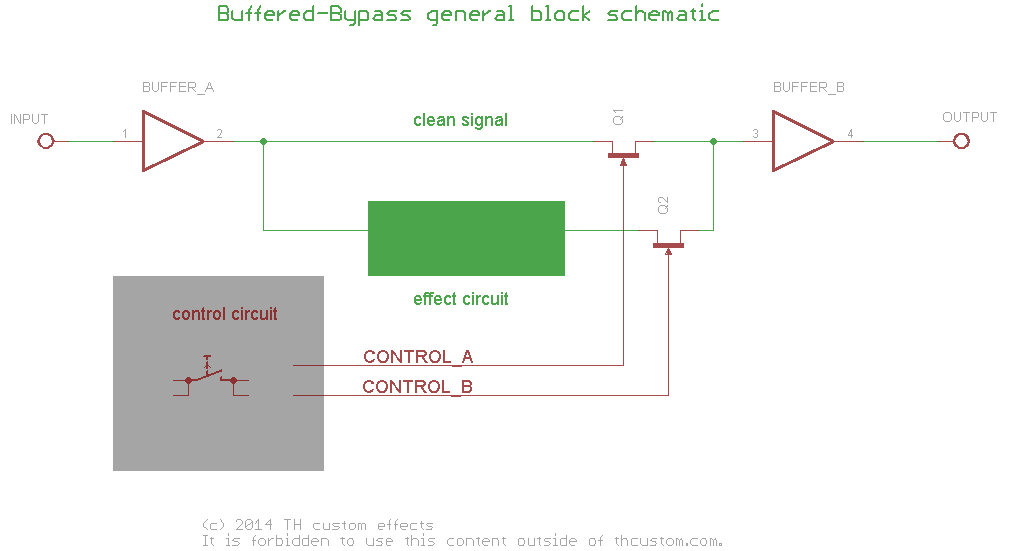
To better understand how the whole thing works here is a block schematic of the major components of an effect pedal.

How it works:
First, the input signal is sent through a buffer. This is important for keeping a high impedance at the input of the effect and having a low impedance output for the signal to be strong enough going through it without major signal loss and deformation.
Second the signal is split into two. The first one (clean signal) passes untouched and is fed into a mixing circuit that is- or is followed by- an output buffer which again makes sure the signal can go a long distance without loosing strenght. The second signal is fed into the effect circuit and what comes out is also going to the mixing circuit.
You also see two JFET transistors hooked into each signal way. They are responsible for doing the signal switching. You see that we need a control signal (two actually) that drive them with opposite states. If the effect is Off, we want to make Q1 conducting (clean signal) and Q2 (effect signal) blocking. If the effect in On, we want Q1 (clean signal) blocking and Q2 (effect signal) conducting.
To reach this goal there is a control circuit which is triggered by a momantary switch and generates both control signals.
The control circuit (analog flipflop)
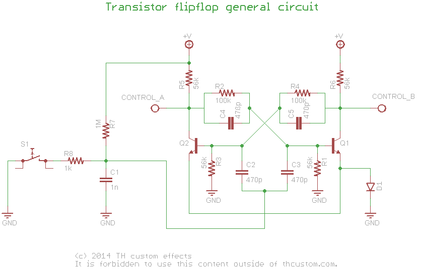
How it works:
The footswitch sends an Off signal to both transistors. As they have opposite states (When Q1 is Off, Q2 is On and vice versa) the one being off already ignores this, but the other transistor will then turn off. The moment it turns off, the opposite transistor will come on. So the momentary impulse toggles the states of this “flip” “flop”.
The missing pieces
We are still missing some details which are shown here.
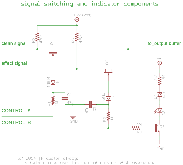
How it works
Each one of the JFET transistors has a few components to help switching the signal. Around Q1 (clean signal) we have R5 which offsets the incoming signal to half of the supply voltage. D1, R1 and C1 make the JFET switching secure and assure that any switching artefacts (spikes) do not harm the components. The same is true for the components around Q2.
In addition to that we see Q3, which is also controlled by CONTROL_B , switching the LED indicator On and Off. The Zener diode brings down the voltage to about 4V (if the effect is powered with 9V) and R4 is the current limiting resistor for the LED.
Guten Abend
Gibt es diesen Bypass fertig aufgebaut ?
Wie schliesst man die Gitarre und 1 Effekt Gerät an die Bypass richtig an ?
Ich freue mich auf Ihre Antwort
Freundliche Grüsse aus der Schweiz
Bruno Keiser
Dieser historische Bypass findet sich in vielen Ibanez und Boss Pedalen der letzten Jahrzehnte. Als eigenständige Einheit gibt es das nicht.